HOTLINE
 Tel: 0510-82391968
 E-mail: James.Wu@jpmechanics.com
 QQ: 1194771942
 Tel: 0510-82391968
E-mail: James.Wu@jpmechanics.com
QQ: 1194771942
Tel: 0510-82391968
E-mail: James.Wu@jpmechanics.com
QQ: 1194771942

 |
|
 |
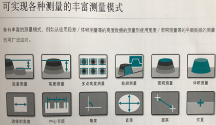 |
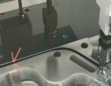
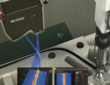
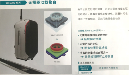
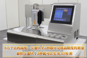
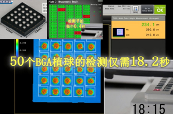
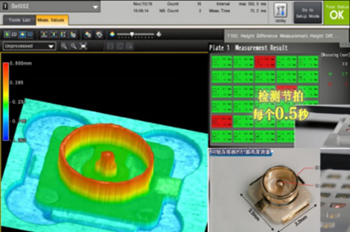
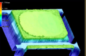
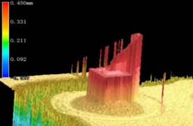
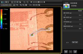
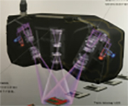
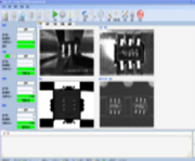
| WI-5000 automatic detector | Case 1:BGA welding ball size detection | Case 2:Connector size detection |
 |
 |
 |
 |
 |
 |
 |
| LED device detection project | Appearance detection of LED devices | Height and coverage of microchip silver pulp | Welding line arc height and quality |
| Serial number | Industry | Picture | WI measurement | WI 3D measurement |
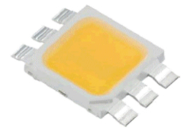
| 1 | LED |  |
 |
 |
| 2 | Welding |  |
 |
 |
| 3 | Copper plate |  |
 |
 |
| 4 | FPC |  |
 |
|
| 5 | Wafer |  |
 |
 |
| 6 | Engraved |  |
 |
 |
| 7 | Coil |  |
 |
|
| 8 | Button |  |
 |
 |
| 9 | Mobile phone frame |  |
 |
 |
| 10 | Gumming |  |
 |
|
| 11 | Chip packaging |  |
 |
 |
| Serial number | Industry | Picture | WI measurement | WI 3D measurement |
| 12 | PCB |  |
 |
 |
| 13 | Hardware components |  |
 |
 |
| 14 | Buzzer |  |
 |
 |
| 15 | Camera |  |
 |
 |
| 16 | Screw hole |  |
 |
 |
| 17 | Building materials surface |  |
 |
 |
| 18 | Camera lens |  |
 |
 |
| 19 | Test paper |  |
 |
 |
| 20 | Gumming |  |
 |
 |
| 21 | Wire harness |  |
 |
 |
| Please contact us for other applications. | ||||
 |
 |
 |
 |
 |
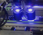
| 3D visual camera | Dual camera system | DB/WB recognition program | Molding decision program | Testing interface |
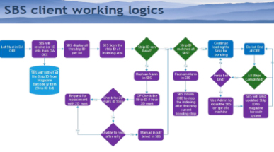
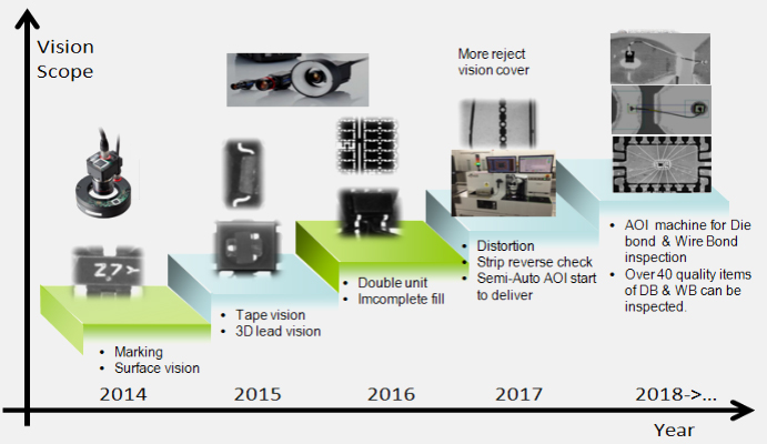
Visual inspection project |
Wafer visual inspection |
DB&WB visual inspection |
Post road visual inspection |
Visual inspection of final test |
| Testing station | The quality of the wafer appearance,wafer sawing |
Die bond |
Molding Electroplating, ball planting, cutting, etc. |
Final Testing |
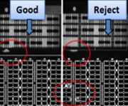
| Detectable content | Wafer size,angle Graphical character Defect detection such as Scratches, Pits Pollution, fragmentation |
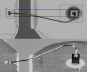
DB:Chip size detection, appearance defect detection, missing, position deflection, flatness, silver paste weight, climb WB:Line arc defects collapse, line break, thread break, tail warping, line skew, line arc too high, leakage welding, etc. |
Molding/Trim/Form:Plastic material is not fully filled, frame distortion, dislocation, chromatic aberration, porosity, damage, pin deformation, product direction, etc. Plating electroplating:During the production process, the location of material and the direction of material installation, location and size of plating are detected. |
Marking lettering:Lettering, inscription, direction, depth Testing:Bend, damage, deflection, device surface defects, scratches, holes, stacking, tilt, direction, etc. |
 Addr: Building 3, sensing equipment Industrial Park, 503 Nanhu Avenue, Wuxi.
 Tel: 0510-82391968
 Fax: 0510-85037168
 E-mail: James.Wu@jpmechanics.com